MRF1570NT1 MRF1570FNT1
7
RF Device Data
Freescale Semiconductor
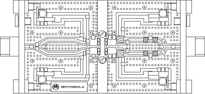
Figure 12. 400 - 470 MHz Broadband Test Circuit Component Layout
C11
B1
C12 C13 C14
C1
C2
C3
C4
C9
C15
R1
C5
C6
R3
R4
R2
C17
B2
C18 C19 C20
L5
L6
C37
C21C23
C22
C24
C42
C26
C25
L1
L2
C27
C34
C28
C39
L3
L4
C29
C30
C32
C33
C38
B5
B6
B3
B4
C35 C36
C40 C41
VDD
GND
VGG
GND
C10
C16
C7
C8
C31
MRF1570T1
Freescale has begun the transition of marking Printed Circuit Boards (PCBs) with the Freescale Semiconductor
signature/logo. PCBs may have either Motorola or Freescale markings during the transition period. These changes will have
no impact on form, fit or function of the current product.
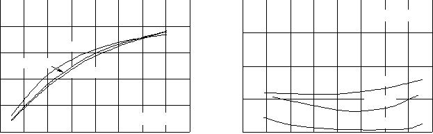
TYPICAL CHARACTERISTICS, 400 - 470 MHz
0
100
0
400 MHz
Pin, INPUT POWER (WATTS)
Figure 13. Output Power versus Input Power
P
out
, OUTPUT POWER (WATTS)
VDD= 12.5 Vdc
80
60
40
20
12345678
440 MHz
470 MHz
80
?20
0
0
Pout, OUTPUT POWER (WATTS)
Figure 14. Input Return Loss versus Output Power
INPUT RETURN LOSS (dB)
IRL,
?5
?10
?15
10 20 30 40 50 60 70
400 MHz
VDD= 12.5 Vdc
440 MHz
470 MHz


发布紧急采购,3分钟左右您将得到回复。
相关PDF资料
MRF18030ALSR3
IC MOSFET RF N-CHAN NI-400S
MRF18060ALR3
IC MOSFET RF N-CHAN NI-780
MRF18085ALSR5
IC MOSFET RF N-CHAN NI-780S
MRF18090AR3
IC MOSFET RF N-CHAN NI-880
MRF19030LSR5
IC MOSFET RF N-CHAN NI-400S
MRF19045LR3
IC MOSFET RF N-CHAN NI-400
MRF19085LR3
IC MOSFET RF N-CHAN NI-780
MRF19090SR3
IC MOSFET RF N-CHAN NI-880S
相关代理商/技术参数
MRF1570NT1_08
制造商:FREESCALE 制造商全称:Freescale Semiconductor, Inc 功能描述:RF Power Field Effect Transistors
MRF1570T1
制造商:FREESCALE 制造商全称:Freescale Semiconductor, Inc 功能描述:RF Power Field Effect Transistors
MRF157MP
制造商:M/A-COM Technology Solutions 功能描述:RF POWER TRANSISTOR MOSFET
MRF158
功能描述:射频MOSFET电源晶体管 5-500MHz 2Watts 28Volt Gain 16dB RoHS:否 制造商:Freescale Semiconductor 配置:Single 晶体管极性: 频率:1800 MHz to 2000 MHz 增益:27 dB 输出功率:100 W 汲极/源极击穿电压: 漏极连续电流: 闸/源击穿电压: 最大工作温度: 封装 / 箱体:NI-780-4 封装:Tray
MRF160
功能描述:射频MOSFET电源晶体管 5-500MHz 4Watts 28Volt Gain 16dB RoHS:否 制造商:Freescale Semiconductor 配置:Single 晶体管极性: 频率:1800 MHz to 2000 MHz 增益:27 dB 输出功率:100 W 汲极/源极击穿电压: 漏极连续电流: 闸/源击穿电压: 最大工作温度: 封装 / 箱体:NI-780-4 封装:Tray
MRF16006
制造商:M/A-COM Technology Solutions 功能描述:TRANS GP BJT NPN 60V 1A 3PIN CASE 395C-01 - Bulk 制造商:M/A-COM Technology Solutions 功能描述:RF POWER TRANSISTOR BIPOLAR/HBT
MRF16030
制造商:MA-COM 制造商全称:M/A-COM Technology Solutions, Inc. 功能描述:RF POWER TRANSISTOR NPN SILICON
MRF161
制造商:ASI 制造商全称:ASI 功能描述:SILICON N-CHANNEL RF POWER MOSFET
